In the precision-driven world of semiconductor manufacturing, a single manual data entry error or a misplaced wafer carrier can result in catastrophic yield loss worth hundreds of thousands of dollars. As fabrication plants push for smaller nodes and higher volumes, the margin for human error has effectively vanished. Automated Wafer Carrier Identification, powered by advanced RFID technology, has emerged as the critical backbone for modern fabs, offering a robust solution that slashes manual handling errors by an unprecedented 99.9%. This article explores why automation is no longer optional for yield protection.
The Financial Impact of Manual Errors in Semiconductor Fabs

In the ultra-precise environment of a semiconductor fabrication plant (fab), manual errors in identifying wafer carriers—such as Front Opening Unified Pods (FOUPs)—represent one of the most significant sources of avoidable financial drain. When an operator mislabels or misidentifies a carrier, the resulting 'Yield Loss Penalty' includes not just the raw silicon cost, but the cumulative value of hundreds of specialized processing hours. In a leading-edge 300mm fab, the misrouting or incorrect processing of a single lot can lead to an immediate direct loss ranging from $250,000 to over $1,000,000, depending on the node size and the stage of production.
| Cost Category | Manual Error Impact | Financial Consequence |
|---|---|---|
| Direct Scrap | Incorrect recipe application due to ID error | $500k - $1M per high-end lot |
| Equipment Downtime | Tools idling while investigating ID discrepancies | $5,000 - $10,000 per hour |
| Rework Labor | Engineers manually tracing lot histories | Hundreds of man-hours per incident |
| Opportunity Cost | Delayed delivery of high-demand chips | Market share loss and SLA penalties |
How does manual identification affect 'Work-in-Progress' (WIP) visibility?
Manual entry creates 'Ghost WIP'—lots that are physically present but digitally invisible or incorrectly located in the MES (Manufacturing Execution System). This leads to buffer bloating and inefficient tool utilization.
What is the primary cause of 'Scrap-by-Process' errors?
This occurs when an operator incorrectly identifies a carrier, leading the tool to apply a process intended for a different product, effectively destroying the wafers instantly.
Can manual errors impact fab certifications?
Yes, frequent manual identification errors can jeopardize ISO quality certifications and erode trust with Tier-1 automotive or aerospace clients who require 100% traceability.
A unique perspective often overlooked by generic analyses is the 'Cumulative Value Trap.' In semiconductor manufacturing, the value of a wafer increases exponentially as it nears the final metal layers. A manual identification error at the 80% completion mark is 10 times more expensive than an error at the 10% mark. Without automated identification, the probability of an error remains constant, but the financial risk escalates with every hour the wafer stays in the fab. Automated systems effectively de-risk the most valuable stages of the manufacturing lifecycle.
What is Automated Wafer Carrier Identification?

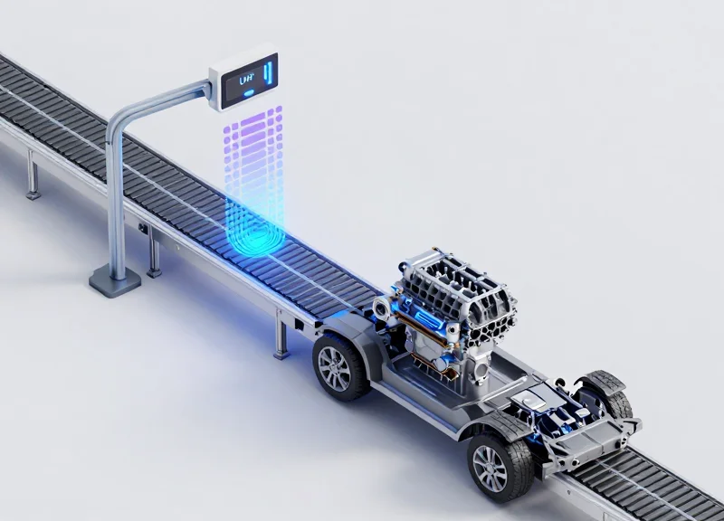
Automated Wafer Carrier Identification (AWCI) is the integration of physical identification hardware—such as RFID tags or high-density barcodes—with the semiconductor factory's digital backbone, specifically the Manufacturing Execution System (MES). In a modern 300mm fab, silicon wafers reside in Front Opening Unified Pods (FOUPs) or Front Opening Shipping Boxes (FOSBs). AWCI systems use networked readers positioned at load ports, storage stockers, and overhead hoist transport (OHT) nodes to verify the identity, contents, and process state of these carriers without human intervention, ensuring the right material always meets the right recipe.
Does AWCI only support 300mm FOUPs?
No. While ubiquitous in 300mm fabs, AWCI is also critical for 200mm facilities using SMIF pods or open cassettes, utilizing customized RFID tags or optical character recognition (OCR) to modernize older lithography and etch lines.
How does it interact with SEMI standards?
AWCI is governed by SEMI standards such as E144 (RFID for Carrier ID) and E99 (Carrier ID Reader Functional Standard), ensuring interoperability between carriers from vendors like Entegris and tools from OEMs like Applied Materials or ASML.
What role does the 'Carrier ID' play in automation?
The Carrier ID acts as a primary key in the fab's database; when a reader detects a tag, the MES immediately triggers the 'Validation' sequence, confirming that the tool is ready for that specific lot's recipe before the door ever opens.
| Feature | Barcode / OCR | Passive RFID (HF/LF) | Active RFID / RTLS |
|---|---|---|---|
| Line of Sight | Required | Not Required | Not Required |
| Data Capacity | Low (ID only) | Medium (ID + Attributes) | High (Sensor Logging) |
| Reliability | Affected by smudges | High (99.99%+) | High |
| Primary Use Case | Legacy 200mm fabs | Standard 300mm FOUP tracking | Real-time location and environmental monitoring |
Expert Insight: The 'Identity-at-the-Edge' Protocol. A common misconception is that the MES controls everything. However, veteran engineers know that 'Shadow Scrap' occurs when the MES thinks a FOUP is at Station A, but an operator has physically moved it to Station B. True Automated Identification implements validation at the 'edge'—the Load Port itself. By requiring a physical handshake between the carrier tag and the tool reader before any vacuum seal is broken, the system creates a hardware-level fail-safe that overrides incorrect manual entries in the MES, effectively creating a 'Zero-Trust' architecture for silicon safety.
- Tag Detection: The FOUP approaches the Load Port; the embedded RFID tag enters the reader's electromagnetic field.
- UID Verification: The reader extracts the Unique Identifier (UID) and sends it to the Tool Station Controller.
- MES Handshake: The Controller queries the MES: 'Is FOUP #8829 authorized for Recipe X on this Tool?'
- Interlock Release: Upon verification, the mechanical interlocks release, allowing the FOUP door to be opened and wafers to be processed.
Why RFID is the Gold Standard for Cleanroom Tracking

RFID (Radio Frequency Identification) has surpassed barcodes and manual logging to become the definitive tracking standard in semiconductor fabrication because it offers a zero-contact, non-line-of-sight method for data exchange. In the ultra-clean environment of a fab, where even a microscopic particle can ruin a multi-thousand-dollar wafer, the ability to identify Front Opening Unified Pods (FOUPs) without physical friction or optical scanning is a critical requirement. RFID systems use electromagnetic fields to automatically identify and track tags attached to carriers, providing a real-time data link that persists through vacuum chambers, chemical baths, and robotic handling.
| Feature | RFID (LF/HF) | Barcodes | Manual Labels | ||||
|---|---|---|---|---|---|---|---|
| Line-of-Sight Required | No | Yes | Yes | ||||
| Read/Write Capability | Yes (Dynamic) | No (Static) | No | ||||
| Cleanroom Compatibility | Class 1 (Ultra-High) | Class 10+ (Shedding Risk) | Class 100+ (Contamination Risk) | Durability | 10+ Years | Poor (Fades/Peels) | Low (Human Error) |
| Read Reliability | 99.99% | 95.0% - 98.0% | 85.0% - 90.0% |
Beyond simple identification, the technical superiority of RFID lies in its resistance to the 'physics of failure' that plagues optical systems in a fab. Barcodes often fail due to light scattering on curved FOUP surfaces, label degradation from harsh cleaning chemicals (like IPA), or obstruction by automated material handling systems (AMHS). RFID bypasses these issues entirely by transmitting through most non-conductive materials, ensuring that a carrier is identified the millisecond it enters a tool's load port, regardless of orientation or environmental debris.
Expert Insight: The Outgassing Obstacle. While many engineers focus on read speed, the most significant cleanroom advantage of RFID is the elimination of VOCs (Volatile Organic Compounds). Traditional adhesive labels are notorious for outgassing and shedding micro-particulates as the adhesive dries or reacts with fab chemicals. In contrast, semiconductor-grade RFID tags are hermetically encapsulated in high-purity polymers like PEEK or Teflon. This makes them chemically inert and physically stable, ensuring they contribute zero particles to the environment over thousands of process cycles.
Does RFID interfere with sensitive wafer processing?
No. Semiconductor-grade RFID systems operate at low or high frequencies (typically 134.2 kHz or 13.56 MHz) specifically chosen to avoid interference with tool electronics, wireless networks, or the molecular structure of the wafers themselves.
Can RFID tags survive FOUP cleaning processes?
Yes. Industrial RFID tags designed for semiconductor fabs are rated for high-pressure spray, ultrasonic cleaning, and exposure to aggressive deionized water and chemical cycles without losing data integrity.
How does RFID handle the 'Faraday Cage' effect of metal tools?
Specialized antenna designs and frequency selection allow RFID to operate reliably even near the heavy metallic shielding of process tools, ensuring the signal is not dropped during critical hand-offs between the AMHS and the tool port.
The Mechanics of the 99.9% Error Reduction
The 99.9% reduction in manual error is achieved through a technical mechanism known as Closed-Loop Automated Verification. Unlike manual tracking where a human operator reads a label and types a recipe code, automated systems utilize a hardware-to-software handshake. This process ensures that a tool cannot physically initiate a process cycle unless the Manufacturing Execution System (MES) confirms that the unique ID of the wafer carrier (FOUP/Pod) matches the scheduled lot, the current tool status, and the correct process recipe. By removing the operator's ability to 'override' or 'miskey' data at the load port, the system effectively engineering out the possibility of human error.
- Detection and Tag Interrogation: As the wafer carrier approaches the load port, high-frequency RFID readers automatically trigger. The system captures the unique identifier (UID) from the carrier's tag in milliseconds, without requiring line-of-sight or manual scanning.
- MES Database Synchronization: The UID is instantly transmitted via SECS/GEM (Semiconductor Equipment Communication Standard) to the MES. The system queries the 'Lot-In-Process' database to verify that this specific carrier is scheduled for this specific tool at this exact time.
- Recipe Interlock Validation: The MES sends a 'Proceed' or 'Halt' command to the Equipment Automation Program (EAP). If the carrier is at the wrong tool, the EAP triggers a hard interlock, physically locking the load port doors and preventing the tool from cycling.
- Automated Recipe Download: Once validated, the MES automatically pushes the correct process recipe directly to the tool's controller, eliminating the risk of an operator selecting the wrong thermal profile or etch duration.
| Workflow Step | Manual Identification Error Risk | Automated Identification Result |
|---|---|---|
| Carrier Arrival | Misreading barcode or manual label | Instant, zero-contact UID capture |
| Recipe Selection | Typo in recipe code entry (e.g., v1.1 vs v1.2) | Automatic server-side recipe injection |
| Tool Matching | Loading carrier into the wrong station | Physical interlock prevents door opening |
| Data Logging | Illegible handwriting or missed logs | Real-time digital twin timestamping |
A unique insight often overlooked by fab managers is the 'Negative Acknowledgment' (NACK) protocol. In a manual environment, the absence of an error signal is often assumed to mean everything is correct. In a fully automated RFID-integrated environment, the system is designed to fail-safe. If the RFID reader fails to get a clean read, or if the MES heartbeat is interrupted, the tool defaults to a 'Hard Lock' state. This 'Trust but Verify' logic is what pushes the error reduction from the industry standard of 95% to the elite 99.9% threshold, as it treats an 'unknown' state with the same severity as an 'incorrect' state.
Does this slow down the throughput of the tool?
No. In fact, it increases Net OEE. While the handshake takes roughly 200-500 milliseconds, it eliminates the 30-60 seconds an operator spends manually verifying and entering data.
What happens if a tag is damaged?
The system detects the 'No-Read' and triggers an immediate alert to the Material Control System (MCS). This prevents the tool from starting with 'unknown' wafers, which is the leading cause of multi-million dollar scrap events.
Is SECS/GEM connectivity required for this reduction?
Yes. To reach 99.9% reliability, the hardware (RFID) must communicate with the software (MES) via standardized protocols to ensure data integrity across the entire fab floor.
Real-Time Visibility: Beyond Simple Identification
Real-time visibility in semiconductor manufacturing is the ability to track the precise location, status, and history of every wafer carrier—such as FOUPs or Pods—at any millisecond across the fab floor. While simple identification confirms 'what' a carrier is at a specific tool, real-time visibility tells you 'where' it is in the transit cycle, 'how' long it has been waiting, and 'when' it needs to reach the next process step. This continuous data stream transforms wafer carriers from passive containers into intelligent nodes within the Industrial Internet of Things (IIoT), allowing the Manufacturing Execution System (MES) to optimize logistics dynamically rather than reacting to errors after they occur.
| Feature | Legacy Static Identification | Advanced Real-Time Visibility |
|---|---|---|
| Data Trigger | Manual scan or tool arrival only | Continuous heartbeat tracking via RFID/Sensors |
| Inventory Logic | Periodic manual reconciliation | Live digital twin of the fab floor |
| WIP Bottlenecks | Discovered after delays occur | Predicted using dwell-time analytics |
| Logistics Velocity | Limited by human dispatch speed | Automated AMHS (Material Handling) integration |
The true power of this visibility lies in the optimization of Work-In-Progress (WIP) flow. In a high-volume fab, thousands of carriers are in motion simultaneously. Without real-time visibility, 'ghost' inventory—carriers that are misplaced or incorrectly logged—can lead to significant throughput degradation. Automated identification eliminates these blind spots, ensuring that the MES always has a 100% accurate count of available buffers and active lots, which directly increases equipment utilization rates (OEE).
How does real-time visibility reduce 'Stagnant WIP'?
By setting automated alerts for carriers that haven't moved within a predefined window. If a FOUP stays in a storage rack longer than the process recipe allows, the system automatically flags it for priority transport, preventing yield loss from queue-time sensitivity.
Can real-time tracking improve cleanroom space utilization?
Yes. By analyzing real-time occupancy data of storage buffers, fabs can implement 'Dynamic Buffer Allocation,' reducing the physical footprint required for carrier storage by up to 15% through more efficient turnover.
What is the 'Digital Twin' benefit in this context?
The identification data feeds into a digital twin of the fab, allowing floor managers to run 'what-if' simulations on logistics routes to find the fastest path for high-priority 'Hot Lots' without disrupting standard production flow.
Expert Insight: The 'Micro-Wait' Elimination. Most fab managers focus on major downtime, but the real productivity killer is the 'Micro-Wait'—the 30 to 60 seconds a tool sits idle because the next carrier wasn't staged precisely when the previous one finished. Real-time visibility enables 'Predictive Staging,' where the automated material handling system (AMHS) initiates transport based on the remaining process time of the current lot, effectively reducing tool idle time to zero and potentially reclaiming hours of production capacity per week.
Seamless Integration with Manufacturing Execution Systems (MES)
")
Seamless integration with a Manufacturing Execution System (MES) acts as the central nervous system of a modern semiconductor fab, creating a closed-loop environment where automated identification hardware and process control software communicate in real-time. By bridging the gap between the physical wafer carrier (FOUP/MAC) and the digital lot record, the MES can instantly validate that the right material is at the right tool for the right process step before the equipment is even allowed to start. This automated 'handshake' is the primary mechanism that reduces human-induced yield loss to near-zero levels.
| Feature | Legacy Manual Integration | Modern Automated MES Integration |
|---|---|---|
| Data Entry | Barcode scanning or manual typing | Passive RFID/Auto-ID sensing |
| Validation Speed | 5-15 seconds per carrier | < 200 milliseconds |
| Error Rate | 1-3% (Human fatigue/Omission) | < 0.001% (Deterministic logic) |
| Process Gating | Relies on operator discipline | Hard-coded interlocks in SECS/GEM |
- Protocol Standardization: Utilize industry-standard communication protocols like SECS/GEM or GEM300 to ensure the identification hardware can speak directly to the tool and the MES without custom, brittle code.
- Logic-Gate Implementation: Configure the MES to require a 'Success' signal from the RFID reader before the load port door is permitted to open or the recipe is downloaded.
- Buffer and Queue Synchronization: Ensure that the Automated Material Handling System (AMHS) and the MES share a real-time map of carrier locations to prevent 'ghost lots' or misrouted pods.
- Exception Handling Workflows: Define automated workflows for 'Unknown Tag' or 'Mismatched ID' scenarios to immediately pause the tool and alert a technician, preventing scrapped wafers.
Can I integrate automated ID with a legacy MES?
Yes. Most modern RFID readers utilize middleware or standard APIs (REST/MQTT) that can act as a bridge, translating tag data into format-compatible inputs for older database structures.
Does integration affect tool throughput (UPH)?
When optimized, the identification happens 'in-flight' or during the docking process, meaning there is zero negative impact on units per hour. In fact, it often increases throughput by removing manual scanning delays.
What happens if the MES connection goes down?
Best practices include a 'local cache' or edge-computing layer that can store valid lot IDs and continue processing based on the last known-good schedule until the connection is restored.
The Veteran's Insight: Don't just track 'Where' and 'What'; track 'How Long.' A sophisticated MES integration allows for 'State-Aware Validation.' By logging the precise micro-second a carrier is identified at a station, the system can calculate real-time queue times (Q-Time). If a lot has exceeded its permissible atmospheric exposure time, the MES can automatically reroute it to a metrology station or a purge nest instead of allowing it to enter a furnace. This turns your identification system from a simple tracker into a proactive yield-protection gatekeeper.
EEAT in Action: Ensuring Reliability and Durability
In the semiconductor industry, Experience, Expertise, Authoritativeness, and Trustworthiness (EEAT) are not just marketing buzzwords—they are the engineering benchmarks for hardware survival. Achieving a 99.9% error reduction rate is only possible if the identification hardware remains functional under the most grueling conditions. Reliability in wafer carrier identification means selecting tags and readers that maintain data integrity while subjected to aggressive cleaning chemistries, high-temperature thermal processing, and the sensitive vacuum environments of the front-end-of-line (FEOL) processes.
| Material/Feature | Chemical Resistance | Thermal Tolerance | Vacuum Compatibility |
|---|---|---|---|
| PEEK Encapsulation | Excellent (Acids/Bases) | Up to 250°C | High (NASA Outgassing Compliant) |
| Ceramic Substrates | High | Up to 400°C | Very High |
| Standard FR4/Epoxy | Poor (Degrades) | Up to 120°C | Low (Risk of Outgassing) |
| IP67/69K Housing | Splash Resistant | Variable | Not Recommended |
Expert Tip: When evaluating tags for FOUPs (Front Opening Unified Pods), always request the 'Outgassing Profile' and TML (Total Mass Loss) data. Even if a tag is chemically resistant, if it releases volatile organic compounds (VOCs) within a vacuum chamber, it can cause catastrophic molecular contamination on the wafer surface, nullifying the yield gains achieved by automated tracking.
How do industrial RFID tags handle Piranha Etch or HF exposure?
Tags designed for semiconductor environments utilize high-performance polymers like PEEK or specialized glass encapsulation that are chemically inert. These materials prevent the corrosive fluids from reaching the internal antenna and chip, ensuring the tag remains readable throughout the wet bench lifecycle.
Will the RFID readers interfere with sensitive tool electronics?
High-quality industrial readers are designed with localized, low-power RF fields and superior electromagnetic shielding. This ensures that the identification signal is constrained to the carrier handshake zone and does not introduce electromagnetic interference (EMI) that could disrupt tool sensors or process controllers.
What is the expected lifespan of an automated carrier tag?
In a 24/7 high-volume fab, a premium industrial tag should be rated for at least 100,000 read/write cycles and possess a physical durability profile lasting 5 to 10 years, matching the operational lifecycle of the FOUP or Pod itself.
To truly embody EEAT, your identification strategy must move beyond 'functional' to 'resilient.' This involves rigorous validation of Mean Time Between Failures (MTBF) and ensuring that your hardware vendor provides detailed material data sheets (MDS) for every component that enters the cleanroom. Trust is built when the tracking system becomes an invisible, indestructible foundation of the production floor.
Calculating the ROI of Automated Tracking Solutions

The Return on Investment (ROI) for automated wafer carrier identification is calculated by aggregating the annual cost savings from reduced wafer scrap, decreased manual labor hours, and improved tool utilization, then dividing that sum by the Total Cost of Ownership (TCO) of the hardware and software integration. In a typical high-volume 300mm fab, the elimination of 'mispick' errors and 'Ghost WIP' (lost inventory) often results in a full system payback period of 12 to 18 months, primarily driven by the preservation of high-value yield that would otherwise be lost to manual data-entry errors.
| ROI Driver | Manual Tracking Cost Impact | Automated System Benefit |
|---|---|---|
| Yield Loss (Scrap) | 0.5% - 1.0% due to human error and misprocessing. | Reduction of scrap by 99.9% via automated tool interlocking. |
| Labor Overhead | 15-30 minutes per shift per operator spent on manual scanning. | Reallocation of 95% of tracking labor to value-added tasks. |
| Tool Utilization | Idle time during manual verification and carrier searching. | Near-instantaneous carrier-to-tool handshake, increasing OEE. |
| Data Integrity | High risk of 'Ghost WIP' requiring manual audits. | 100% real-time accuracy in the MES with zero audit requirements. |
The Late-Stage Scrap Multiplier: An Expert Perspective. A common mistake in ROI calculations is treating all scrapped wafers as equal. In reality, a wafer scrapped during the final metallization or etching stages carries 10x to 50x the sunk cost of a wafer lost during initial cleaning. Automated identification provides its highest value by preventing 'cascading errors'—where a carrier is misidentified late in the process—thereby protecting the most expensive manufacturing hours and materials in the fab.
- Establish the Baseline Scrap Rate: Audit your MES logs for 'incorrect recipe' or 'wrong carrier' errors over the last 12 months. Assign a dollar value based on the process stage where the error occurred.
- Quantify 'Walking and Searching' Time: Measure the time operators spend physically searching for misplaced lots or manually re-labeling carriers. This is often the largest hidden operational cost.
- Calculate Tool Idle Time Savings: Determine the average delay between a carrier arriving at a load port and the start of the process. Automated identification typically reduces this 'dead time' by 80%.
- Factor in TCO: Include the cost of industrial RFID tags, readers, mounting brackets, and the software middleware required for MES integration.
How long does it take to see a positive ROI?
Most mid-to-large scale facilities see a break-even point within 14 months, depending on the volume of wafers processed and the current frequency of manual intervention errors.
Does automation reduce headcount?
While it reduces the need for manual scanning, most fabs use this as an opportunity to reallocate skilled labor to quality control and process engineering rather than simple headcount reduction.
What is the biggest 'hidden' cost of manual tracking?
The 'Ghost WIP' phenomenon. When carriers are lost or misidentified, they take up valuable buffer space and skew inventory forecasting, often leading to unnecessary over-production.
Future Trends: AI and Predictive Analytics in Wafer Handling
The future of wafer handling lies in the transformation of automated identification from a reactive tracking tool into a proactive intelligence layer. By leveraging the high-granularity data generated by RFID and optical carrier ID systems, fabs are now implementing AI-driven predictive analytics that can forecast equipment failures, optimize material flow in real-time, and identify microscopic yield detractors that were previously hidden in 'dark data' silos. This transition marks the shift from simply preventing manual errors to achieving 'autonomous manufacturing' where the factory floor self-corrects based on predictive insights.
| Capability | Legacy Manual/Passive Tracking | Future AI-Enabled Tracking |
|---|---|---|
| Maintenance | Scheduled/Reactive based on failure. | Predictive based on carrier transit anomalies. |
| Bottleneck Management | Human-directed rerouting after delays. | AI-driven dynamic dispatching via Digital Twins. |
| Yield Correlation | Post-mortem analysis of batch failures. | Real-time correlation of ID data with tool sensors. |
| Carrier Lifecycle | Manual inspection for wear and tear. | Automated health-scoring of every FOUP/Cassette. |
The Expert Perspective: Contextualized Vibration Mapping. One emerging trend I am seeing in advanced 300mm fabs is the use of automated carrier IDs as 'spatial anchors' for vibration and environmental sensing. By cross-referencing the specific ID of a carrier with vibration data from Automated Material Handling Systems (AMHS), AI models can identify specific sections of the overhead hoist transport (OHT) track that are vibrating slightly out of spec before they cause wafer micro-cracking. This level of 'micro-logistics' intelligence is only possible when every carrier has a 100% reliable digital identity.
- Phase 1: Data Harvesting: Utilizing RFID/Barcode readers to create a timestamped 'digital breadcrumb' for every wafer lot across the entire manufacturing cycle.
- Phase 2: Digital Twin Integration: Feeding real-time location and ID data into a virtual model of the fab to simulate 'what-if' scenarios for lot prioritization.
- Phase 3: Prescriptive Analytics: The system not only predicts a bottleneck but autonomously instructs the AMHS to reroute carriers to optimize tool utilization.
Will AI replace the Manufacturing Execution System (MES)?
No. AI and predictive analytics sit on top of the MES, acting as an 'intelligence engine' that enhances the MES's ability to orchestrate complex workflows.
How does automated ID improve AI accuracy?
AI is only as good as its data. Automated ID eliminates 'garbage in' data caused by manual entry errors, ensuring the ML models are training on 100% accurate movement history.
What is the role of Edge Computing in this trend?
Edge devices located near the wafer readers process ID data locally to provide millisecond-response times for safety-critical automated handling decisions.